The increasingly developing era of industrial intelligence has increasingly stringent requirements on sensor performance, volume, weight and cost. AKUSENSE's precision optoelectronic series products are known for their long detection range, long detection range, fast response speed and high precision. How to achieve this? What about more extreme photoelectric performance? It all starts from this [core] world~
In fact, to realize the functions of precision optoelectronics, traditional technology is realized through discrete components, but this has many disadvantages: the more discrete components, the larger the size of the PCB board, poor anti-interference ability, poor consistency, temperature Problems such as rapid rise and affected lifespan ensue.
So, what if dedicated integrated circuits are used to replace traditional discrete electronic components?
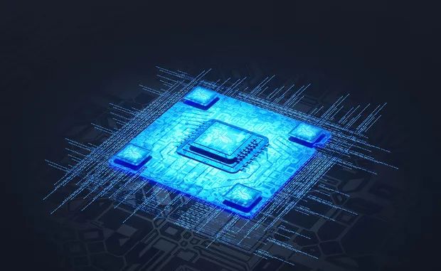
What is an application specific integrated circuit?
Application-Specific Integrated Circuit: ASIC (Application-Specific Integrated Circuit)
ASIC chips, as application-specific integrated circuits, are designed for specific needs and have the characteristics of high integration, low power consumption and excellent performance, so they play a key role in industrial sensors. Specifically reflected in the following points
1. Highly integrated: Through chip design, photoelectric sensors can achieve smaller size and lighter weight, which facilitates their easy embedding into various electronic devices. At the same time, the chip uses large-scale integrated circuit technology, which can integrate more functions and circuits and improve the integration and performance of the sensor.
2. Performance improvement: Chip design helps to enhance resistance to EMC interference and improve the sensitivity and accuracy of photoelectric sensors. Photoelectric sensor chips utilize the interaction between an internal photosensitive electrode and an external light source. When light shines on the photosensitive electrode, photons interact with the photosensitive material to generate a voltage signal. This design enables the photoelectric sensor to accurately measure small changes in light intensity.
3. Optimize data processing: The processing circuit inside the chip can amplify and convert the collected signals to obtain accurate light intensity or optical power information. At the same time, the realization of high-speed data processing and storage capabilities also relies on the integrated circuit design inside the chip, which is crucial for applications in fields such as optoelectronic control, measurement, and communications.
In fact, the development cost of ASIC is quite high, which makes it possible to realize the value of its investment only in large-scale production. However, with its extensive product line, Meiji Sensing is able to provide customers with more diverse solutions, especially in those extremely challenging application scenarios, we can still ensure stable detection results.
More extreme product performance has always been our unremitting goal. Therefore, we resolutely chose the road of independent development of ASIC to meet the needs of the market and customers.
By using ASIC chip technology and the chip's high integration, stability and scalability, we have achieved a good start ahead of the market and can continue our technological leadership through it.